
Last Update: 2019-07-21
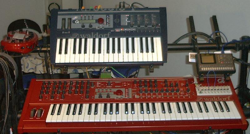
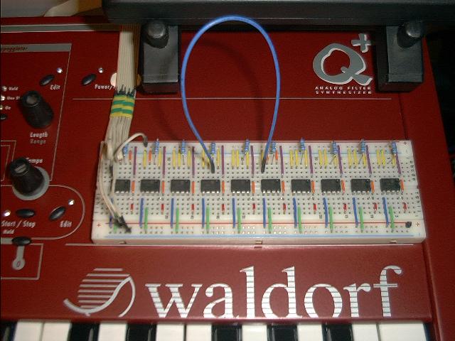
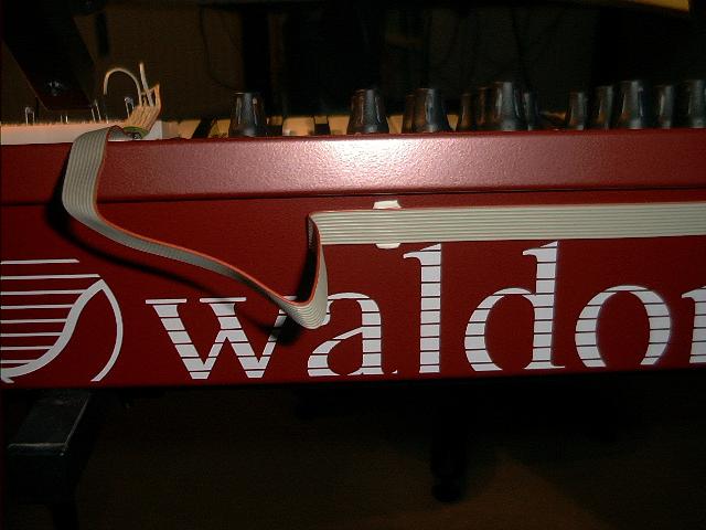
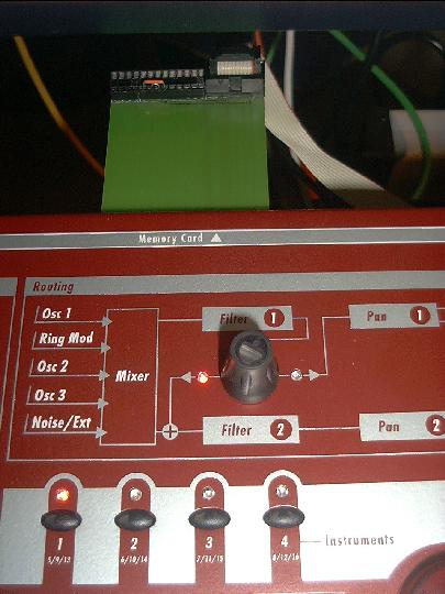
HomeDownloadsTuning and TemperamentDIY StuffGear PicsI use QCards very often, but I tend to have the wrong one inserted and it's awkward to keep many of them around while working on the Q because I never find enough places where I can put them (if you look closely, you'll find three QCards in this picture JPEG 63k). So I made this BigQCard JPEG 53k that serves well as ten QCards. I select the card (actually a 24LC256 from Microchip, available for instance from Farnell) I'm going to use with the blue jump wire and I can write protect any card by inserting the red bridges in a different way. The actual connection to the Q is made by a ribbon cable JPEG 38k that attaches to an adapter JPEG 38k that I bought from MAKI. Everything is attached with something called »MultiFix« that resembles chewing gum very closely. This stuff is quite strong and holds the parts nicely, but it will peel off without a trace if necessary.
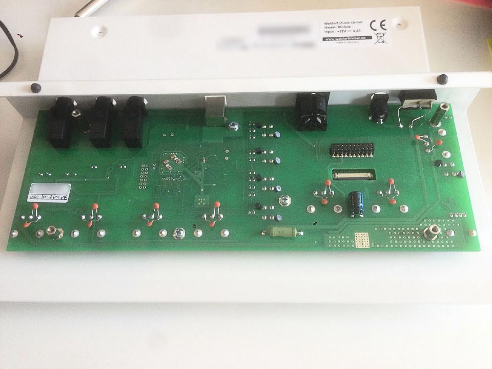
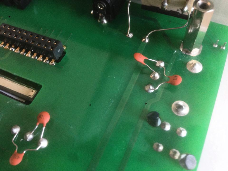
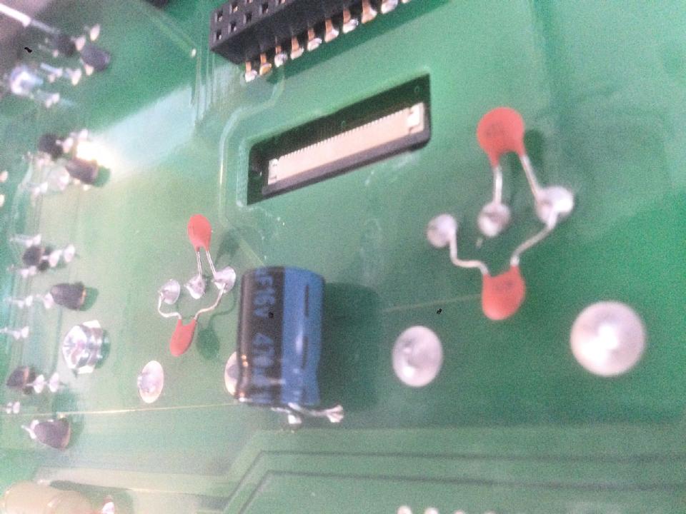
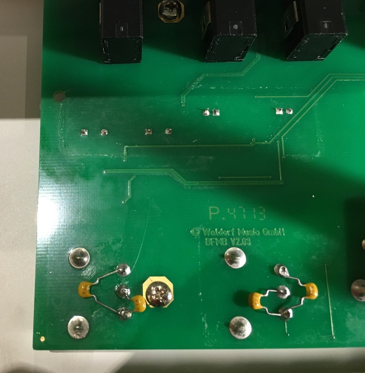
It has been reported that the rotary encoders on some gear »wear out« quickly and need to be replaced. When the encoders on my desktop Blofeld started to behave erratically, I've had a closer look — there was no way they could have worn out already and had not been subjected to any adverse environmental conditions. As a quick look with the scope would show, they simply bounced a bit longer than the software likely expected and the line to the controller seemed to pick up noise while the contacts were open. Now there's a much easier fix for that than outright replacing the encoders (which probably creates the same problem again in a few months): bypass the contacts with a small capacitor to prevent the controller picking up the noise and mis-interpreting it as encoder movement. There's a pair of contacts in each encoder and I've added a bypass to ground for each contact. I've settled for 470pF C0G, the value is not overly critical, but should probably not be much larger than about 1nF. SMT caps size 0805 fit perfectly between the encoder pins, while a piece of wire provides the ground connection. SMT caps are a bit tricky to solder by hand, so you could use leaded caps instead, they are just a bit more expensive in small quantity and you should watch out a carefully that the leads won't short anything.
JPEG 90k JPEG 92k JPEG 102k JPEG 82k
Yes I know, I should not have used the flash on these pictures, but the work area just wasn't lit well enough on this day to take them with the flash switched off. Encoder operation has been smooth ever since this modification. My other Blofeld never had this problem to start with, so I left it un-modified.
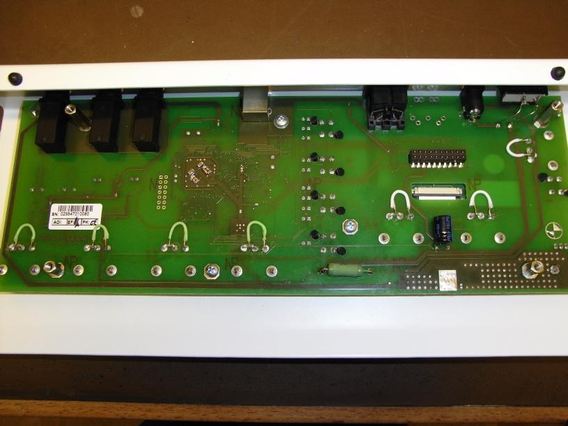
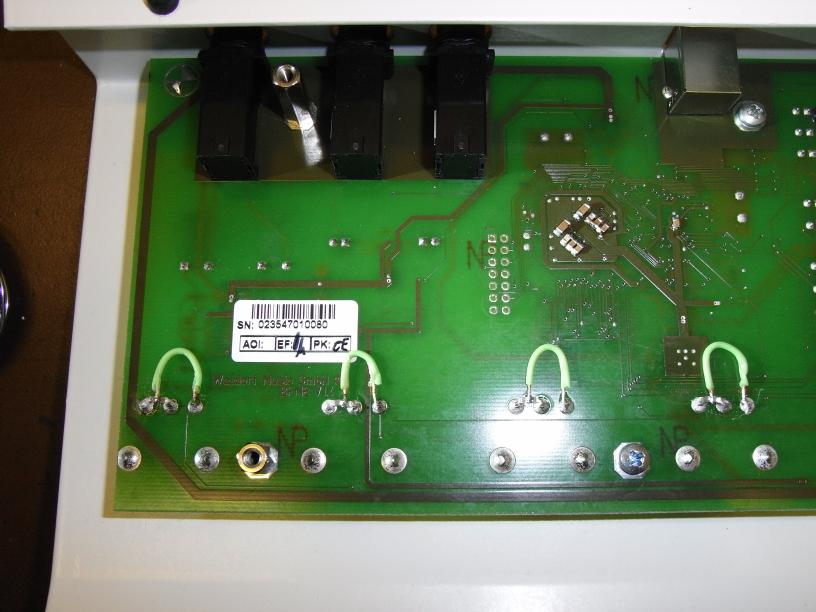
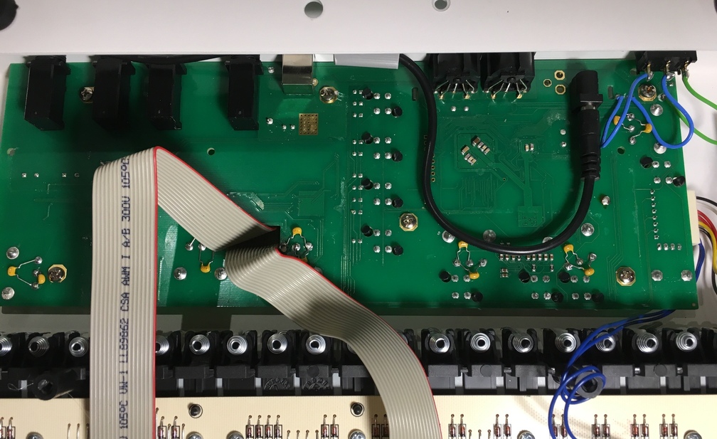
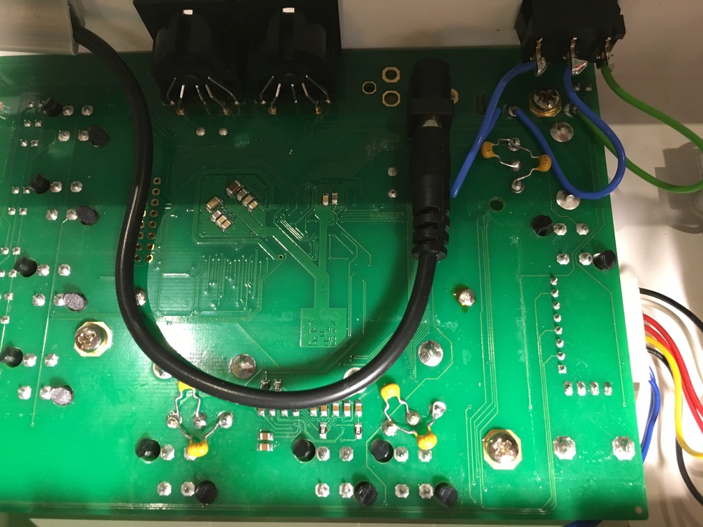
Here's a picture of the fix done with leaded caps, so you can see how to connect things in that case. Thank you Gary!
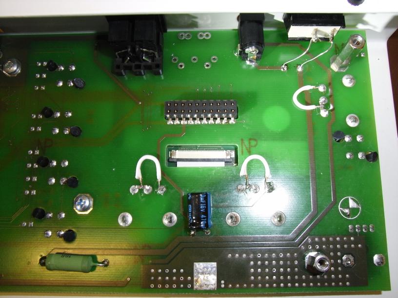
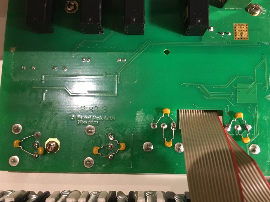
Here are some more pictures of the fix done with leaded caps, thank you Jonas!
JPEG 69k JPEG 76k JPEG 90k JPEG 90k
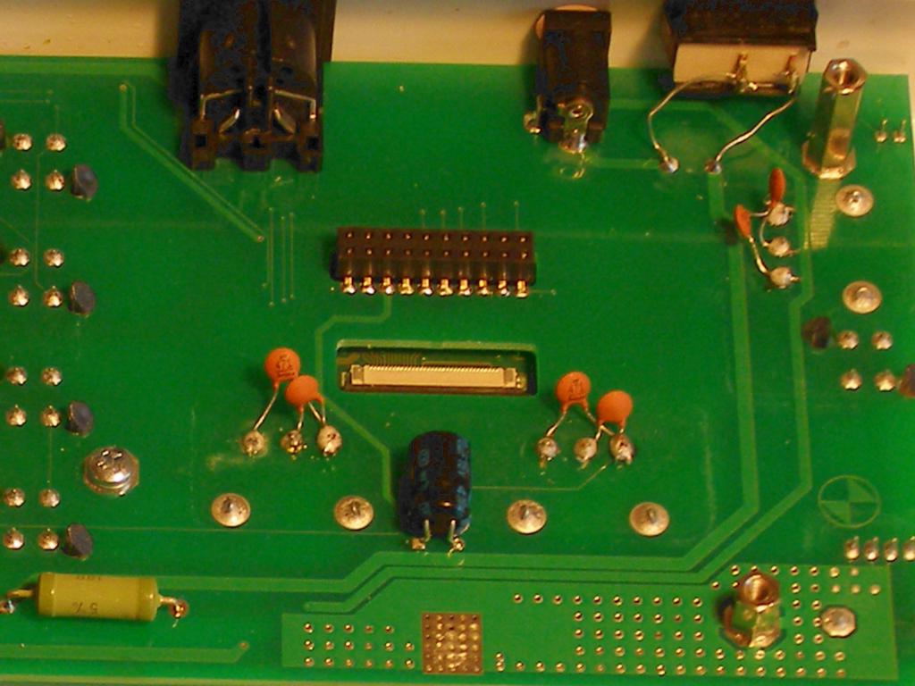
Here are some more pictures of the fix done with leaded caps on a Blofeld Keyboard, thank you Anthony!
JPEG 236k JPEG 180k JPEG 220k JPEG 240k
Here's a paper in progress on the OTA PDF 410kiB. I plan to expand on that in various directions: temperature dependence analysis and applications. Corrections and suggestions are welcome (last update: July 2008).
A VCO can be built with a dual-slope integrator. If the currents for the up- and down-slope integration are appropriately controlled, then the symmetry (ratio of upward and downward slope) of the wave can be modulated without changing the frequency. This paper PDF 181kiB derives the necessary equations and gives a sketch of a circuit implementing them.
To check out the freeware version of Cadsoft Eagle, I've designed a 32x32 switch matrix based on the AD75019 16x16 crosspoint switch IC from Analog Devices. This version allows only two signal layers and a board size of half-Eurocard format (80mm x 100mm), which limited the board design quite a bit. Download this Eagle project ZIP 60k and unpack in your Eagle project folder. There's a few notes in the DESCRIPTION file in that folder that Eagle will display when you click on the project in the Control Center, if you don't have Eagle, simply load it into your web browser. The Board layout PDF 249k and the Schematics PDF 201k are seperately available (you don't need to download these if you have Eagle).
I've since re-thought the layout issues coming from the limitations of the Freeware version and how to actually build and assemble the thing. The result is a new board layout for just one switch matrix chip PDF 86k corresponding to these very simple schematics PDF 75k, the Eagle files are included in the project ZIP above. By using different pin headers, any number of these boards can then be combined to form various switch topologies. One of the motivations of doing a sub-board is of course that you can re-use them if you should later decide that you'd need a different configuration. Stay tuned for a 32x32 version using this board as a building block...
You would need at least a controller to feed the information on which switches are closed into the matrix to do anything with this. Some wires that hang off a serial or parallel port on a PC would be good enough for starters, I envisioned the matrix to be controlled via MIDI by something like a PIC and to be used as a cordless audio patch panel in front of my mixer. For synth audio/CV switching, you will probably want to add I/O buffering and programmable gain. Be aware that the shift register in those chips is dynamic, so there is a lower boundary to the clock for this operation. It would not be fun to inject 1024 bits with hand-operated switches anyway. If you (want to) do anything with this, please let me know.
It has long been known that the CEM chips used in so many synthesizers were semi-custom IC. Doug Curtis, just out of college, had won a design contest sponsored by Interdesign (later sold to Ferranti/GEC Plessey) and went on to work for Interdesign before founding Curtis Electromusic Specialties, later to fold into OnChip Systems. The founder of Interdesign and designer of the '555 timer chip, Hans Camenzind, still operates consultancy business in mask programmable analog semicustom IC, Array Design and has written the book Designing Analog Chips that is available free for download or as a print-on-demand hardcopy.
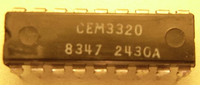
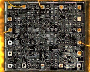
Here are the first two pictures of de-encapsulated (defect) CEM chips, more to follow as time permits. While any Interdesign or Ferranti die marks are missing, it is obvious that these are bipolar arrays. Comparison of the actual chips with a databook »201 Analog IC Designs« from Ferranti GmbH (1980) yields a perfect match, so any doubts about the true nature of these two CEM chips can be put to rest. I have in the meantime been able to also obtain an earlier brochure »101 Analog IC Designs« from Interdesign and their »Designer's Handbook« (sic) for Monochip A to D with the layout sheets for Monochip A to C and some issues of »Monogram«. While not directly applicable to the Monochip arrays used by the CEM chips, these have been helpful in corroborating some of the finer details of the chip micrographs. Many thanks to those who've helped in tracking them down.
If anybody happens to have a Design Manual for these bipolar arrays (Monochip D to M) or the 200x layout sheets thereof, please get in touch with me. I'm also interested in any other Interdesign literature.
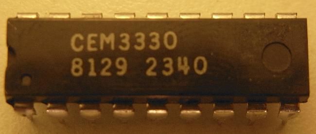
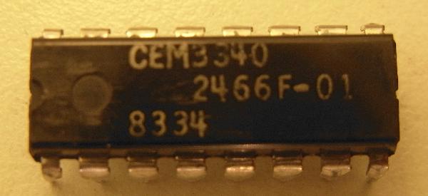
| Type | CEM3310 | CEM3320 | CEM3330/CEM3335 | CEM3340/CEM3345 |
|---|---|---|---|---|
| Datasheet | PDF 2.8MiB | PDF 3.1MiB | PDF 3.4MiB | PDF 3.6MiB |
| Package | JPG 20kiB | JPG 19kiB | JPG 20kiB | JPG 19kiB |
| Chip | JPG 24kiB | coming soon | coming soon | JPG 32kiB |
| Date | CW36/1983 | CW47/1983 | CW29/1981 | CW34/1983 |
| Code | 1985(A) | 2430A | 2340 | 2466F(-01) |
| Size (mils) | 70x70 | N/A | N/A | 77x88 |
| Size (mm) | 1.8x1.8 | N/A | N/A | 2.0x2.2 |
| Interdesign/Ferranti Monochip® type | MOE (confirmed) | N/A | N/A | MOH (confirmed) |
The datasheets show chips from the first week of 1979 for the CEM3310, while the CEM3340 in the datasheet is three weeks older than the specimen on display here. Both the MOE and MOH have internally 18 pins, and both have 17 bonds. The CEM3340 very likely is just a bond variant of the CEM3345, which has one more ground pin and an open emitter square wave output. This is most likely the pad without bond, while the extra bond is a ground connection just as it is in the CEM3345.